
Launches three new solutions, designed for students studying semiconductor research, development, and manufacturing
Keysight Technologies, Inc. (NYSE: KEYS) today announced three new semiconductor teaching lab solutions designed to help universities prepare students for careers in the global semiconductor industry. The three solutions—Basic Design and Measurement, Parametric Test and On-Wafer Measurement, and Photonics IC Measurement—provide students with practical experience using professional-grade tools and workflows that are commonly used in semiconductor research, development, and manufacturing.
This press release features multimedia. View the full release here: https://www.businesswire.com/news/home/20260324805653/en/
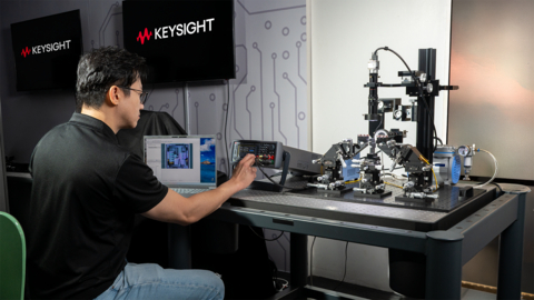
Keysight’s semiconductor teaching lab solutions give students hands-on experience with industry-standard semiconductor test tools and workflows.
As the semiconductor industry accelerates globally, universities face increasing pressure to produce graduates who are industry‑ready. Academic institutions recognize that theory alone is no longer sufficient, and students must gain hands‑on experience with the same measurement techniques, workflows, and tools used in real semiconductor R&D and manufacturing environments.
Keysight addresses this challenge by providing solutions designed for training and development. As part of this effort, Keysight delivers a structured, progressive learning pathway that mirrors real-world semiconductor test workflows. Students gain hands-on experience setting up professional measurement hardware, performing fundamental electrical tests, device characterization, and photonic IC characterization using industry-standard equipment with guided lab modules.
Key benefits include:
- Hands-on training with industry-standard semiconductor instruments, measurements, and workflows.
- Structured lab modules that help students connect textbook concepts to real-world semiconductor applications.
- A learning approach that aligns theory with practice and prepares students for professional engineering careers.
Lim Han Sing, Vice President, General Electronics Measurement Solutions at Keysight Technologies, said: “Both educators and the wider industry play a critical role in developing the next generation of semiconductor engineers. By bringing real-world measurement techniques into the classroom, Keysight is helping educators deliver practical, job-relevant training that aligns closely with industry needs. This move will bridge the gap between education and practical experience, supporting the future workforce.”
Resources
- Product Page: UU101LAB Basic Design and Measurement
- Product Page: UU102LAB Parametric Test and On-Wafer Measurement
- Product Page: UU103LAB Photonic IC Measurement
About Keysight Technologies
At Keysight (NYSE: KEYS), we inspire and empower innovators to bring world-changing technologies to life. As an S&P 500 company, we’re delivering market-leading design, emulation, and test solutions to help engineers develop and deploy faster, with less risk, throughout the entire product life cycle. We’re a global innovation partner enabling customers in communications, industrial automation, aerospace and defense, automotive, semiconductor, and general electronics markets to accelerate innovation to connect and secure the world. Learn more at Keysight Newsroom and www.keysight.com.
View source version on businesswire.com: https://www.businesswire.com/news/home/20260324805653/en/
Contacts
Keysight Media Contacts
Andrea Mueller
Americas
andrea.mueller@keysight.com
Fusako Dohi
Asia
fusako_dohi@keysight.com
Jenny Gallacher
Europe
jenny.gallacher@keysight.com
If you believe this article contains misleading, harmful, or spam content, please let us know.
Report this article